B.Tech. III Semester
Examination, June 2024
Grading System (GS)
Max Marks:
70 | Time: 3 Hours
Note:
i) Attempt any five questions.
ii) All questions carry equal marks.
a) Explain the operation of a bistable multivibrator built around IC 555. Also, briefly discuss one of its applications in the field of digital systems. (Unit 4)
b) Explain the operation of a Schmitt trigger using IC 555 with a neat and labelled diagram. (Unit 4)
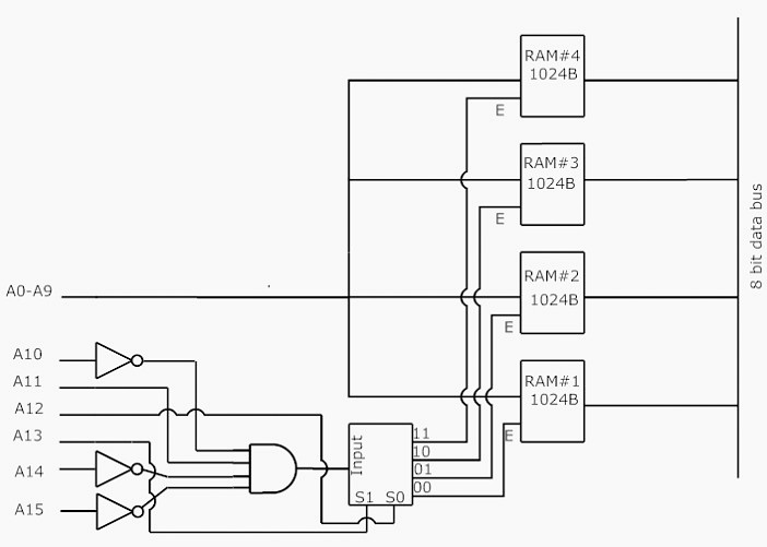
a) There are four chips each of 1024 bytes connected to a 16-bit address bus as shown in Fig. 1, given below. Find the address mapping of RAMs 1, 2, 3 and 4 respectively. (Unit 3)
b) Explain the operation of a dual slope type ADC with a neat and labelled diagram. (Unit 4)
a) Realize the Boolean function $F (A, B, C) = \Sigma(1, 3, 4, 5, 6, 7)$ using only minimum number of 2-to-4 line decoder to generate the function at a particular output pin of decoder. (Unit 2)
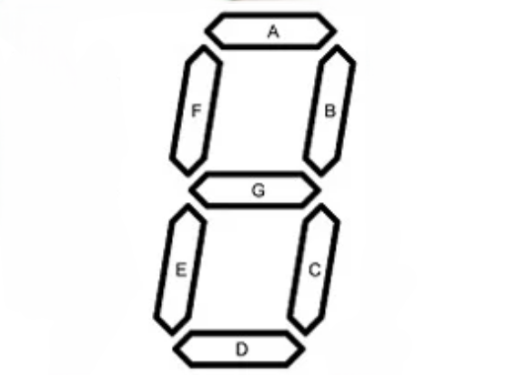
b) A digital circuit which converts a BCD to seven segment is to be designed. A typical seven segment LED is shown in Fig. 2 given below. Design the logic circuit for the segment 'C' only. Assume the LED glows, when the input to segment is logic 'HIGH'. (Unit 2)
a) For the circuit shown in Fig. 3, identify the implemented Boolean logic expression for output 'Y'. (Unit 4)

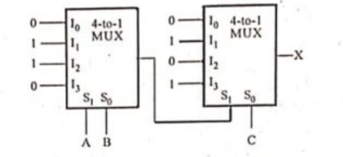
b) Find the output expression for variable 'X' for the given logic circuit shown in Fig. 4. (Unit 2)
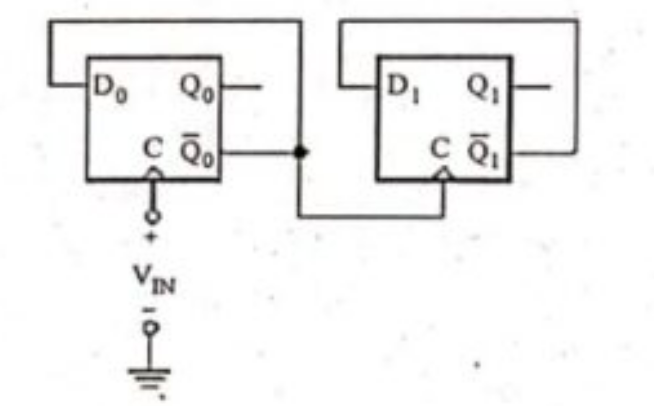
a) The D flip-flops of Fig. 5 are positive edge triggered. Assuming that prior to t = 0, the states are $Q_0 = 0$ and $Q_1 = 0$, sketch the voltage waveforms at $Q_0$ and $Q_1$ versus time. Assume logic levels of 0 V and 5 V. (Unit 3)
b) Explain the operation of a 4-bit R-2R ladder DAC using a neat diagram. (Unit 4)
a) Draw the truth table of a 2-bit by 2-bit binary multiplier. Implement the same using half adder and required additional logic gates. (Unit 2)
b) Design a MOD - 4 synchronous UP counter using JK flip-flop. (Unit 3)
a) Explain BPSK modulation scheme. (Unit 5)
b) What do you understand by time division multiplexing? (Unit 5)
a) What is pulse code modulation? Explain about the quantization and quantization error. (Unit 5)
b) Explain Nyquist sampling theorem. What should be typical sampling frequency for sampling a sinusoidal signal of frequency (Fm, Hz) for a practical system? (Unit 5)